Nikon
NSR 2205 i 14 E 2 i-Line
The Nikon NSR 2205 i 14 E 2 is an i-line stepper. The NSR 2205 i 14 E 2 uses an i-line light source.[1][2][3][4][5]

What it is
How it works
General reference — not yet source-verifiedIn an i-line stepper, the photomask (reticle) is illuminated by the i-line source, and a reduction lens projects a scaled image of the mask pattern onto a resist-coated wafer. The wafer is mounted on a precision stage that steps to each exposure field, repeating the exposure across the entire wafer. The step-and-repeat process enables high overlay accuracy and consistent critical dimension control.
Where it fits in the process flow
General reference — not yet source-verifiedUpstream processes include wafer cleaning, deposition, and resist coating. Downstream processes include post-exposure bake, resist development, pattern inspection, and transfer into the underlying film by etching or ion implantation.
What do the numbers mean?
Wafer handling1
Optics & imaging4
Performance2
Control & software2
Configuration & options26
- Asahi N 4 A-C Chamber:[1]
- Set Temperature:[1]
- Alpha Station[1]
- HP Alpha Alpha Server DS 15 A[1]
- HP Alpha Server DS 15 A[2]
- Asahi N 4 Z Chamber:[3]
- Asahi N 4 A-B Chamber:[4]
- Smart Modular Technology[4]
- ETM 25 SA[4]
- Nikon Nest[5]
- Fully Refurbished[9]
- Chamber
- Asahi N 4 A-C (2006 unit), Asahi N 4 A-C (2001 unit), Asahi N 4 Z (2008 unit), Asahi N 4 A-B (2001 unit), Asahi N 4 A-C (2001 unit)[1]
- MCSV Version
- 3.46 C (2006 unit), 3.46 D (2001 unit), 3.46 D (2008 unit), 3.43 C (2001 unit), 3.43 C (2001 unit)[1]
- Vintage
- 2006 (unit 137809), 2001 (unit 137808), 2008 (unit 137807), 2001 (unit 137806), 2001 (unit 137805)[1]
Vintage & configurations
Documented models & variants
| Designation | Generation | Vintage | Changes | Source |
|---|---|---|---|---|
| NSR 2205 i 14 E 2 | i-Line | 2001–2008 | Sources show different listed vintages and configurations across entries, including Asahi N 4 A-C or Asahi N 4 Z chamber, different computer types, and MCSV versions 3.43 C, 3.46 C, and 3.46 D. | Equipment inventory listing[5] |
What replaced it?
Alternatives
Tools documented as functional equivalents — same process step and wafer size, from a different manufacturer. Each equivalence cites its source.
- ASML PAS 5500— Same function class: Lithography, 200mmCompare in depthsource[10]
Where are the manuals?
Generated from public-source data on file. Enter your email to access — nothing is published; details are routed privately.
Not publicly documented
Field notes
No research found yet — worked with this tool? Share what you know.
Frequently asked questions
How does a stepper maintain overlay accuracy across multiple layers?General reference — not yet source-verified
Overlay accuracy is maintained through an alignment system that reads marks on the wafer and on the reticle. The stepper uses these marks to align each die position relative to previously patterned layers. Feedback from the alignment system continuously corrects the wafer stage position, and the baseline of the projection lens is periodically calibrated to compensate for drift.
What are the routine maintenance requirements for such a system?General reference — not yet source-verified
Routine maintenance includes periodic cleaning of optical surfaces, calibration of the alignment system, and replacement of the mercury lamp bulb at the end of its operational life. The system also requires regular inspection of the wafer stage, vacuum systems, and environmental controls to ensure consistent performance. The manufacturer provides a maintenance schedule and procedures to minimize downtime.
What is the typical throughput of an i-line stepper?General reference — not yet source-verified
Throughput is determined by several factors, including exposure field size, resist sensitivity, wafer handling speed, and the number of alignment steps. While exact throughput depends on the specific configuration and process parameters, this class of stepper is generally designed for high-volume production and can process a significant number of wafers per hour under optimized conditions.
Not publicly documented
The following facts about the NSR 2205 i 14 E 2 i-Line are absent from this record as of this revision. First-hand knowledge or a citation closes a gap; every submission is reviewed before publication.
No publicly documented production dates or lifecycle milestones (introduction, end of production, EOL) for the NSR 2205 i 14 E 2 i-Line are on record.
Answerable by: OEM historical records or a trade-press announcement
The control-system platform and OS era of the NSR 2205 i 14 E 2 i-Line are not on record.
Answerable by: an engineer who operated it or OEM installation records
No publicly documented failure modes or field errata for the NSR 2205 i 14 E 2 i-Line are on record.
Answerable by: a field service engineer, process engineer, or maintenance technician
The process node or technology generation of the NSR 2205 i 14 E 2 i-Line is not on record.
Answerable by: an OEM datasheet or a fab qualification report
No publicly documented compatible parts, consumables, or accessories for the NSR 2205 i 14 E 2 i-Line are on record.
Answerable by: an OEM parts catalog or a service engineer
No research found yet — worked with this tool? Share what you know.
Sources & citations
Sources (10)Every fact above is drawn from these public sources
- [1]inventory listing
- [2]inventory listing
- [3]inventory listing
- [4]inventory listing
- [5]inventory listing
- [6]Inventory photo
- [7]Inventory photo
- [8]Inventory photo
- [9]inventory listing
- [10]nist.govnist.gov
Last updated Oct 1, 2026.
Compare with similar tools
View all →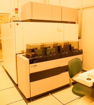
The ASML PAS 5500/275D is a high-throughput i-line stepper with 5X reduction, 365 nm exposure, and automated wafer handling for substrates up to 200 mm diameter.
The GCA AutoStep 200 DSW (also known as AS200) is a 5X reduction i-line wafer stepper designed for up to 200mm wafers.
The SUSS MicroTec BA8 Gen4 Pro is a semi-automated mask alignment and wafer bonding system for 200 mm wafers, with capabilities including exposure, UV bonding, fusion bonding, imprinting, and selective plasma activation.