Heidelberg Instruments
MLA150
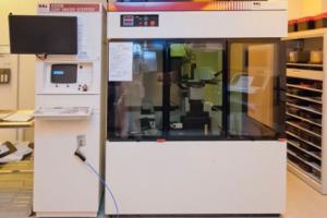
The Heidelberg Instruments MLA150 is a mask-less aligner (direct-write lithography system) that exposes photoresist directly on a substrate using a UV laser (375 nm or 405 nm) without the need for a physical mask. The MLA150 achieves a minimum feature size of 1 µm. The MLA150 can also achieve feature sizes down to 600 nm.[1][2]

Plate 01Heidelberg MLA150 Training - Pritzker Nanofabrication Facility
Anna MukhortovaWatch on YouTubePlate 02Multilayer lithography with the Maskless Aligner MLA150
Nano Vacuum Pty LtdWatch on YouTubePlate 03Photolithography without a mask: Multilayer lithography with the Maskless Aligner MLA 150
Heidelberg InstrumentsWatch on YouTubePlate 04Extract from EPFL User Interview: MLA 150 at the Center of MicroNanoTechnology (CMi) at EPFL
Heidelberg InstrumentsWatch on YouTubePlate 05MLA 150 Anniversary – Gregg Moore Shares a Story
Heidelberg InstrumentsWatch on YouTubePlate 06ASU Core Facilities Equipment Showcase: Heidelberg MLA 150
Arizona State University ResearchWatch on YouTubePlate 07MLA 150 Anniversary – Steffen Diez on How It All Began
Heidelberg InstrumentsWatch on YouTube
What it is
The Heidelberg Instruments MLA150 is a maskless aligner manufactured by Heidelberg Instruments GmbH. The system uses laser diodes at wavelengths of 375 and 405 nanometers. The MLA150 accommodates substrates up to 220 millimeters square and provides a maximum exposure area of 150 by 150 millimeters. Alignment accuracy is specified as less than 500 nanometers.[1][2][4]
How it works
The MLA150 employs a digital micromirror device to spatially modulate the exposure light from a laser source. The system uses interferometer-based position control for the moving stage. Autofocus is achieved through combined optical and pneumatic sensors that monitor the distance to the substrate surface. The MLA150 supports both topside and backside alignment through dedicated optics.[1][4]
Applications
Application areas for the MLA150 include life sciences, MEMS, micro-optics, semiconductor fabrication, sensors, actuators, MOEMS, and materials research involving nanotubes and graphene. The system can produce high-aspect-ratio features in thick photoresist and three-dimensional topography through grayscale mode.[2][1][4]
- Direct writing of patterns onto wafers
- Fast patterning of masks and wafers
- Life Science
- MEMS
- Micro-Optics
- Semiconductor
- Sensors
- Actuators
- MOEMS
- Material Research
- Nano-Tubes
- Graphene
Why won't it start?
Documented failure modes, common issues, and field considerations.
- The source states a risk of crashing the writehead on small chips if the loading procedure is not followed accurately.
- The source states the equipment is sensitive to airborne solvent contamination on optical elements.
- The source states the sample must contain at least a 5 x 5 mm square for pneumatic autofocus to work correctly.
What do the numbers mean?
Wafer handling22
Optics & imaging33
Performance6
Control & software1
Configuration & options17
Vintage & configurations
Documented models & variants
| Designation | Generation | Vintage | Changes | Source |
|---|---|---|---|---|
| MLA150 - 1 | — | — | Listed as one of the MLA150 system entries; source provides separate specifications for this unit. | epfl.ch[1] |
| MLA150 - 2 | — | — | Listed as one of the MLA150 system entries; source provides separate specifications and grayscale/high aspect ratio options for this unit. | epfl.ch[1] |
| MLA150-1 | — | — | Maximum substrate size 220 x 220 x 8 mm; 375 nm laser power 2800 mW; writing time with 375 nm laser on a 100 mm wafer is < 32 min (Fast mode). | epfl.ch[1] |
| MLA150-2 | — | — | Maximum substrate size 200 x 200 x 12 mm; 375 nm laser power 7200 mW; writing time with 375 nm laser on a 100 mm wafer is < 9 min (Fast mode); includes high aspect ratio and grayscale lithography features. | epfl.ch[1] |
What replaced it?
Alternatives
Tools documented as functional equivalents — same process step and wafer size, from a different manufacturer. Each equivalence cites its source.
- SUSS MicroTec ACS 200 +— Same function class: Lithography, nullCompare in depthsource[6]
Related models
- siblingHeidelberg Instruments VPG200— The source mentions the MLA150 as another Heidelberg laser writer installed in the CMi clean room; the Himt convert interface is similar for both. The MLA150 is mentioned as an alternative for exposing AZ10XT at 405 nm, which is forbidden on the VPG200.source[5]
Where are the manuals?
Publicly hosted documents referencing this tool, linked at their original location. Hosted by the linked institutions — availability may change.
- UG07 Conversion Software Guide (APP) - MLA 150 [01424].pdfDocumentumd.edu
- UG08 Design Creation Guide - MLA 150 [01424].pdfDocumentumd.edu
- UG11 Grayscale Guide - MLA 150 [01424].pdfDocumentumd.edu
Generated from public-source data on file. Enter your email to access — nothing is published; details are routed privately.
Not publicly documented
Field notes
No research found yet — worked with this tool? Share what you know.
Frequently asked questions
What is the minimum resolvable feature size?
The MLA150 can achieve minimum feature sizes down to approximately 0.4 micrometers with thin photoresist, and features of 1 micrometer are readily obtained.[4][1]
Not publicly documented
The following facts about the MLA150 are absent from this record as of this revision. First-hand knowledge or a citation closes a gap; every submission is reviewed before publication.
No publicly documented production dates or lifecycle milestones (introduction, end of production, EOL) for the MLA150 are on record.
Answerable by: OEM historical records or a trade-press announcement
The control-system platform and OS era of the MLA150 are not on record.
Answerable by: an engineer who operated it or OEM installation records
The process node or technology generation of the MLA150 is not on record.
Answerable by: an OEM datasheet or a fab qualification report
No publicly documented compatible parts, consumables, or accessories for the MLA150 are on record.
Answerable by: an OEM parts catalog or a service engineer
Sources & citations
Sources (9)Every fact above is drawn from these public sources
- [1]epfl.ch — epfl.chepfl.ch
- [2]pnf.uchicago.edu — pnf.uchicago.edupnf.uchicago.edu
- [3]cns1.rc.fas.harvard.edu — cns1.rc.fas.harvard.educns1.rc.fas.harvard.edu
- [4]wiki.nanotech.ucsb.edu — wiki.nanotech.ucsb.eduwiki.nanotech.ucsb.edu
- [5]epfl.chepfl.ch
- [6]web.archive.orgweb.archive.org
- [7]UG07 Conversion Software Guide (APP) - MLA 150 [01424].pdf — nanocenter.umd.edunanocenter.umd.edu
- [8]UV direct write [HEIDELBERG-MLA] | Quantum-Nano Fabrication and Characterization Facility | University of Waterloo — uwaterloo.cauwaterloo.ca
- [9]Systemingenieur (m/w) für Laserlithographie-Systeme — himt.de (Aug 25, 2019)web.archive.org
Last updated Oct 8, 2026.
Compare with similar tools
View all →
The SUSS ACS 200 + is a coater and developer for semiconductor wafer processing, handling 6-inch or 8-inch wafers.
The GCA 6300 DSW is a g-line wafer stepper used for lithography, with source descriptions also identifying related i-line GCA 6300 stepper documentation.
The MA / BA Gen4 Pro Series is a semi-automated mask aligner and bond aligner system supporting wafers up to 150 mm / 200 mm, with capabilities for exposure, UV bonding, fusion bonding, micro- and nanoimprinting, and selective plasma activation.
