SPTS
APS
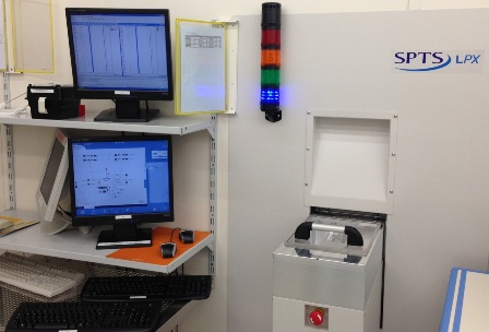
The SPTS APS (Advanced Plasma System) is an inductively coupled plasma (ICP) based high density plasma source. The SPTS APS was optimized for etching dielectrics including SiO2, SixNy, SiC, and Al2O3. The SPTS APS features independent wafer voltage biasing from the ICP and electrostatic clamping.[1]
What it is
The SPTS APS is an inductively coupled plasma (ICP) etching system. The system was optimized for etching dielectric materials such as silicon dioxide, silicon nitride, silicon carbide, aluminum oxide, and various glasses. The SPTS APS is used for etching dielectrics that are difficult to etch using conventional RIE or ICP sources.[1]
Where it fits in the process flow
General reference — not yet source-verifiedIn semiconductor fabrication, dielectric etch tools such as the SPTS APS are used to transfer patterns into dielectric layers after photolithographic patterning. The etched dielectrics may then serve as insulating layers, passivation layers, or sacrificial layers. In MEMS and photonics fabrication, the system can be used to etch thick dielectric substrates such as fused silica or Pyrex.
Applications
The SPTS APS is used for etching a variety of dielectric materials. For silicon dioxide etching, recipes using C4F8/He or C4F8/H2/He yield etch rates from 170 to 440 nm/min with selectivity to photoresist from 2.8:1 to over 25:1. For silicon nitride, a CHF3/SF6 recipe provides etch rates of 160-220 nm/min with selectivity of 2:1 against photoresist. Polyimide is etched using oxygen with etch rates up to 1300 nm/min. Fused silica and Pyrex are etched with C4F8/O2 using aluminum masks, with etch rates of 760 nm/min and 580 nm/min respectively. Lithium niobate wafers are etched with CHF3/Ar using a chromium mask with an etch rate of 90 nm/min.[1]
- Etching dielectrics such as SiO2, SixNy, SiC, Al2O3, and glass types
What do the numbers mean?
Power & electrical2
Wafer handling8
- Stated processes
- BARC_Slow, Si3N4_Smooth, SiO2_PR_1:1, SiO2_PR_2:1, SiO2_PR_3:1, SiO2_PR_3:1_SOFT, SiO2_PR_5:1, SiO2_PR_soft, Pi_vertical, Pi_tapered, Fused_silica, Pyrex, LiNbO3_wafers, Chamber clean[1]
- Chuck temperature
- 10 °C for most processes, 20 °C for fused silica, 25 °C for Pyrex, -10 °C for LiNbO3[1]
Gas & chemistry3
Optics & imaging2
Control & software1
Configuration & options9
- Maximum etch time
- 20 minutes for processes marked with *; longer etches are split into steps with an automatic O2 dry clean between each[1]
What replaced it?
Related models
- siblingAlcatel AMS 200 SE— Listed in the same etching equipment section.source[2]
- siblingTokyo Electron Unity Me— Wafers processed in the SPTS APS etcher are not allowed in the TEL Unity etchersource[3]
What does it need to run?
Site utility requirements, footprint, and infrastructure needed to install and operate this tool. Sourced from public records.
- Gases availableO2, Ar, CHF3, He, C4F8, SF6, H2[1]
- Available gasesO2 (0-100 sccm), Ar (0-100 sccm), CHF3 (0-100 sccm), He (0-500 sccm), C4F8 (0-100 sccm), SF6 (0-100 sccm & 0-500 sccm), H2 (0-50 sccm)[1]
- Wafer voltage biasingIndependent from the ICP[1]
- Wafer biasWafer voltage biasing independent from the ICP[1]
- Process gasesO2 (0-100 sccm), He (0-500 sccm), SF6 (0-100 sccm), H2 (0-50 sccm), plus Ar, CHF3, C4F8[1]
Where are the manuals?
Generated from public-source data on file. Enter your email to access — nothing is published; details are routed privately.
Not publicly documented
Field notes
No research found yet — worked with this tool? Share what you know.
Frequently asked questions
What gases are available on the SPTS APS?
The available gases are O2 (0–100 sccm), Ar (0–100 sccm), CHF3 (0–100 sccm), He (0–500 sccm), C4F8 (0–100 sccm), SF6 (0–100 sccm and 0–500 sccm), and H2 (0–50 sccm).[1]
How is endpoint detection performed?
Endpoint detection can be performed by optical emission spectroscopy (EOS) or by laser reflectometry/interferometry. For oxide etching, the 440 nm spectral line corresponding to SiF is used. For cleaning, the multi-region 685–695 nm lines corresponding to COx are used.[1]
What is the maximum allowed leak-up-rate for wafer cooling?
The leak-up-rate (LUR) must not exceed 200 mTorr per minute to ensure correct cooling of the wafer.[1]
What materials can be etched with the SPTS APS?
The system is optimized for etching dielectrics including SiO2, Si3N4, SiC, Al2O3, glass types, polyimide, fused silica, Pyrex, and LiNbO3.[1]
What is the etch rate for fused silica?
The etch rate for fused silica using a C4F8/O2 recipe with an aluminum mask is 760 nm/min with selectivity greater than 12:1 against the mask.[1]
Not publicly documented
The following facts about the APS are absent from this record as of this revision. First-hand knowledge or a citation closes a gap; every submission is reviewed before publication.
No publicly documented production dates or lifecycle milestones (introduction, end of production, EOL) for the APS are on record.
Answerable by: OEM historical records or a trade-press announcement
No publicly documented variants, configuration options, or revision breakpoints of the APS are on record.
Answerable by: an OEM product catalog or an engineer who ordered or specified the tool
The control-system platform and OS era of the APS are not on record.
Answerable by: an engineer who operated it or OEM installation records
No publicly documented failure modes or field errata for the APS are on record.
Answerable by: a field service engineer, process engineer, or maintenance technician
The process node or technology generation of the APS is not on record.
Answerable by: an OEM datasheet or a fab qualification report
No research found yet — worked with this tool? Share what you know.
Sources & citations
Last updated Oct 8, 2026.
Compare with similar tools
View all →The Applied Materials 0010-47763 is an electrostatic chuck (ESC) assembly used in semiconductor etching processes.
The Applied Materials 0010-16392 is an electrostatic chuck assembly designed for 300 mm wafer processing, featuring a dual electrode configuration.
Oxford Instruments 100 ICP Fluorine is an inductively coupled plasma etcher for fluorine-based etching, supporting cryo DRIE and multiple etch gases including SF6 and C4F8.
